Technology
Since its establishment, Gpixel has adhered to the development principle of independent research, independent innovation, and has continuously broken through the technical difficulties in the key areas of high-performance CMOS image sensors. Gpixel has formed a series of core technologies with completely independent intellectual property rights in the areas of pixel design, circuit design and process development.
Global Shutter
Global shutter sensors simultaneously expose all pixels on the sensor and read them out in a sequential, line-by-line manner. This approach offers several advantages, particularly in high-speed applications where a rolling shutter could lead to image distortions or skew. The global shutter is essential for capturing accurate images of moving objects, such as items undergoing inspection on a production conveyor belt. Gpixel boasts an extensive product range featuring charge domain Global Shutter technology, delivering excellent performance characterized by low noise and high shutter efficiency.
Large Area Design
Gpixel's image sensor chips are often featuring large pixel size (up to 16 um) or large resolution (up to 152MP), often exceeding the maximum printable size of a reticle during the lithography steps of wafer fabrication. Consequently, producing a single chip with such dimensions requires multiple lithographic exposures called stitching. To address this challenge, we divide the sensor design into smaller blocks and generate sensors by replicating these blocks. Our advanced 1D/2D stitching technology ensures precise alignment of these blocks, enabling the manufacturing of large-area sensors with both high yields and exceptional performance.
High Speed and HDR
Gpixel employs various strategies to enhance the conversion speed, including the utilization of multiple ADCs distributed across the top and bottom of each column. Additionally, we employ 3D stacking to shorter in-chip connections, further expediting the conversion and read out process and boosting frame rates. Gpixel's sensor technology incorporates innovative approaches such as dual-gain readout from the same exposure, which not only speeds up conversion but also achieves higher dynamic ranges of up to 90-100 dB. Furthermore, in advanced chip architectures with wafer stacking, on-chip fusion of these multiple gain readout images is made possible, allowing for even greater versatility and performance.
Time Delay Integration
In scenarios characterized by low light conditions combined with short exposure times, Time Delay Integration (TDI) sensors can significantly enhance signal-to-noise ratios by accumulating the exposure charge from multiple lines that are synchronously exposed in response to relative motion of the object under inspection. At Gpixel, our CCD-in- CMOS technology effectively blend the strengths of CCD and CMOS technologies, producing exceptional outcomes with our TDI image sensors at high line rates of up to 1 MHz.
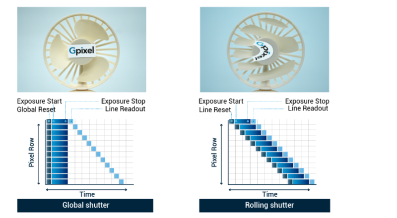
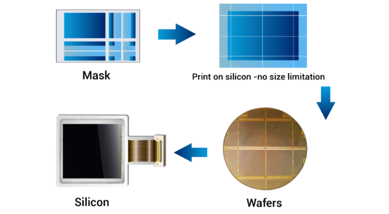
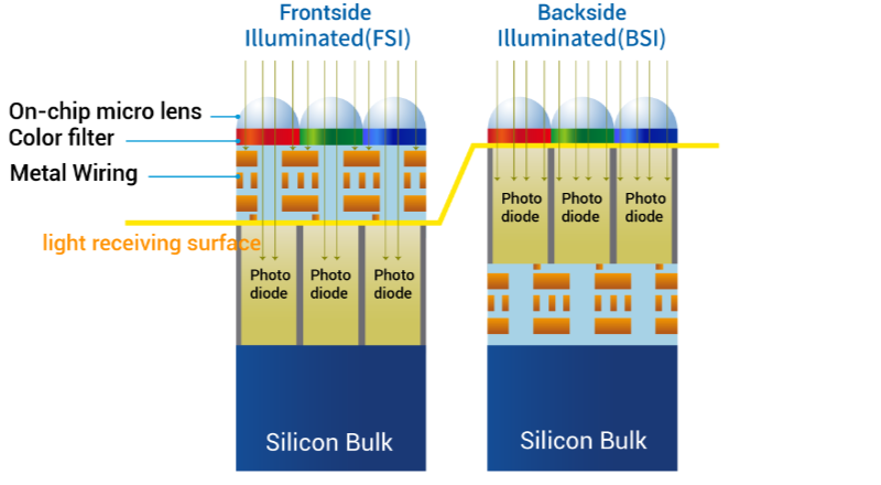
Back Side Illumination
In a conventional image sensor, the photodiodes are integrated onto the silicon substrate, with the metal interconnects positioned above them. Consequently, some light gets reflected, reducing the amount of light that ultimately reaches the photosensitive layer. A back-side illuminated (BSI) sensor uses a manufacturing technique which involves flipping the silicon wafer and thinning its reverse side, allowing light to directly reach the photocathode layer without traversing through the metal wiring layer. This renders BSI sensors exceptionally well-suited for applications where superior low-light performance is essential, such as in industrial sensors, security cameras, microscope cameras, and astronomy systems. Moreover, BSI sensors offer an optimal solution for detecting non visible energy such UV light down to soft x-rays.
3D Wafer Stacking
The classic monolithic approach integrates both the analog pixel array and the control and readout digital logic onto a single IC, offering clear advantages but also posing challenges in terms of performance and real estate optimization. Enhancing the performance of pixel and analog components may not align with optimizing digital logic effectively. The 3D stacking process involves bonding two wafers together, with one typically containing the pixel and some analog circuits and the other housing the digital logic. This inherently incorporates a backside illuminated pixel layer. This approach allows for independent optimization of each layer, effectively addressing conflicting requirements. Furthermore, this architecture enables advanced readout and conversion rates, further boosting frame or pixel rates.
Copyright © 2023 Gpixel Microelectronics Inc. All rights reserved Legal Notices Cookies Policy Privacy Policy Site Map
0