GL Series
The GL sensor family from Gpixel comprises a wide range of horizontal resolutions, ranging from 2k to 16k, with line rates of up to 200 kHz. These sensors feature pixel sizes of 3.5 µm, 5 µm, 7 µm, and 14 µm, providing a comprehensive selection to suit diverse line scan applications.
Global Shutter
High Speed
TDI
High Resolution
GLT5016BSI
16k BSI TDI (TIME DELAY INTEGRATION) LINE SCAN IMAGE SENSOR
GLT5016BSI is a Backside illuminated (BSI), Time delay integration (TDI), charge domain CMOS image sensor with 5 μm pixels and 16416 effective resolutions. The sensor has two photosensitive bands, 256 stages and 32 stages respectively enabling a high dynamic range (HDR) imaging mode, which is designed to meet the needs of high speed and low light applications by maximizing sensitivity with state-of-art BSI scientific CMOS technology. GLT5016BSI Sensor integrates an on-chip sequencer, supports channel multiplexing and selectable 2 scan directions (Forward and Reverse). It is assembled in a 415 pins μPGA ceramic package for reliability and good heat dissipation. GLT5016BSI comes in 2 spectrum variants: an UV-optimized with high QE below 300 nm and a visible and NIR range optimized version.
  • Key Features and Benefits

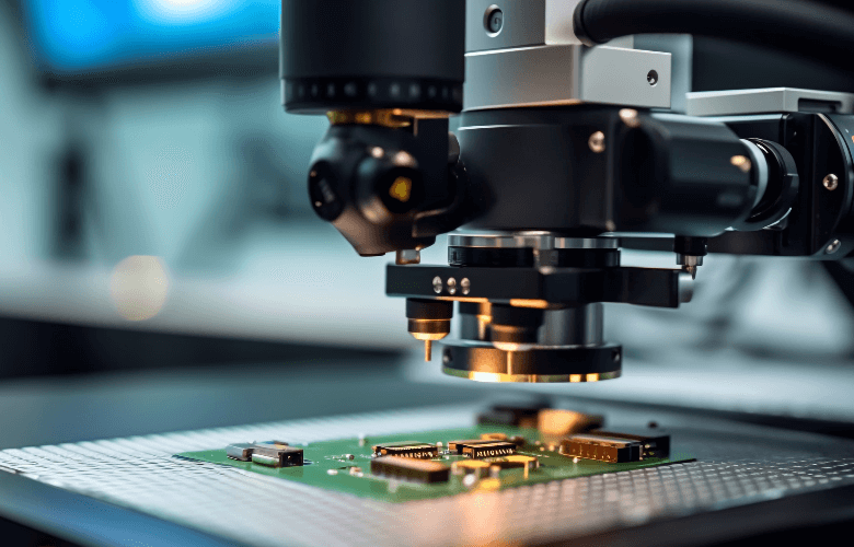
    True Charge Domain Time Delay Integration

    Back Side Illuminated (BSI) pixels

    High Sensitivity with QE of 70.7% (266 nm)(UV Version) and up to 92.4 % (440 nm)(VIS version)

    High Speed: up to 500 kHz

    HDR Read Out

    On-chip Binning

  • Package Drawing
  • QE Curve
GLT5016BSI
GLT5016BSI
Specifications
  • Resolution

    16.4K

    Nr of Active Pixels

    P1: 16416 pixels x 256 stages P2: 16416 pixels x 32 stages

  • Optical Format

    82.02 mm

    Pixel Size

    5 μm x 5 μm

  • Full Well Capacity

    15.2 ke‾

    Temporal Noise

    7.5 e‾

  • Dynamic Range

    66.1 dB

    Max Line Rate

    500 kHz

  • Peak QE

    UV version: 70.7% (266 nm), 87.8% (420 nm) VIS version: 92.4% (436 nm), 87.0% (590 nm)

    Shutter Type

    Time Delay Integration

  • Photosensive Area

    P1: 82.08 mm × 1.28 mm P2: 82.08 mm × 0.16 mm

    Dark Current

    0.97 ke‾/pix/sec (15℃)

  • Max. SNR

    41.7 dB

    ADC

    12 bit

  • Output Format

    108 ch Sub-LVDS

    Channel Multiplexing

    108/96/72/48/36/24/12

  • Max. Data Rate

    103.68 Gbps

    Chroma

    Mono

  • Power Consumption

    < 6.6 W

    Supply Voltage

    3.3 V (analog) 1.65 V (ADC) 1.6 V (digital)

  • Package

    μPGA 415 pins (98.08 mm x 19.00 mm)

    Availability

    Engineering Samples (ES)

Product Number
  • GLT5016BSI-ABM-NUN-BUE
    VIS version.415 pins μPGA package.Sealed D263® Teco glass lid with AR coating on both sides,ES
  • GLT5016BSI-AUM-NUN-BRE
    UV version.415 pins μPGA package.Removable D263® Teco glass lid with AR coating on both sides,ES
  • GLT5016BSI-ABM-NUN-BUD
    VIS version.415 pins μPGA package.Sealed D263® Teco glass lid with AR coating on both sides,Demo Grade
  • GLT5016BSI-AUM-NUN-BRD
    UV version.415 pins μPGA package.Removable D263® Teco glass lid with AR coating on both sides,Demo Grade
Download
Flyer
Datasheet
Application
Subscribe
You will instantly receive the latest information about this product's update.
Copyright © 2025 Gpixel Microelectronics Inc. All rights reserved Legal Notices Cookies Policy Privacy Policy Site Map
Contact Us
  • Name *

  • Company Name *

  • Country/Region *

  • Email *

  • How can we help? *

I agree to receive the latest products and technical consultations from Gpixel (can be unsubscribed at any time).

I have read in detail and agree to Gpixel's Privacy Policy

  • Please click on the verify
  • 0