

 date:2024-01-29
January 29, 2024, Changchun, China – Gpixel announces the GSENSE3243BSI CMOS image sensor, the first product to incorporate GSENSE 2.0 technologies for high-throughput, high-dynamic range, and high-sensitivity scientific imaging.
GSENSE3243BSI is the first sensor in the GSENSE product family to be built in advanced 65 nm CMOS process technology, using 3D wafer stacking techniques with backside Illuminated pixels, and incorporating per-pixel on-chip memory, a combination of technologies that defines the new generation of scientific image sensors from Gpixel.
The state-of-the-art wafer stacking technology used in the GSENSE3243BSI sensor allows the BSI pixel array to be designed on a separate silicon wafer than its read-out circuit, pushing optical performance and read-out speeds beyond what is possible on single chip architectures. The BSI pixels in the top wafer are fully optimized for maximum light sensitivity and low noise performance. The bottom digital CMOS wafer contains an array of core cells each supporting a high speed 14-bit ADC circuit and SRAM memory blocks which are used to seamlessly sum and store up to 4 subsequent sub-frames.

Fig. 1 Advanced 3D wafer stacking technology allows the backside illuminated pixel array to be optimized for sensitivity while the overall architecture is optimized for throughput and dynamic range.
“With this combination of cutting-edge technologies, we can offer scientific grade sensors with exceptional dynamic range and throughput, meeting the needs of the growing biosciences instrumentation market,”says Wim Wuyts, Gpixel’s Chief Commercial Officer.
GSENSE3243BSI is a 8192 x 5232 resolution image sensor with a 3.2 μm2 pixel and 31.1 mm diagonal. The full resolution of the sensor can be read out at a bit depth of 14 bits and a maximum frame rate of 100 fps using an on-chip high-speed serial interface or at 50 fps over 32 sub LVDS channels operating at 1.05 Gbps/channel. Additionally, on-chip binning and flexible ROIs can be used to achieve higher frame rates at lower resolutions.
The sensor incorporates multiple features to enhance dynamic range including the dual-gain output popular with the first generation of GSENSE products. The sensor also incorporates an on-chip compression HDR function which prioritizes the most important bits of data for each pixel, and a digitally programmable piecewise linear HDR feature. The sensor achieves a dynamic range of 75 dB in dual gain mode and up to 104 dB using the more advanced HDR features. Unique to GSENSE 2.0 products is the ability to use the on-chip SRAM to seamlessly add up to 4 exposures, thereby increasing the photodiode capacity by a factor of 4. In the GSENSE3243BSI image sensor, this enables an in-pixel full well charge of up to 96 ke- in full resolution and 192 ke- in 2x2 binning mode. These various options make it possible to detect small signal deviations in biosciences applications where background luminescence challenges the performance of traditional sCMOS image sensors.
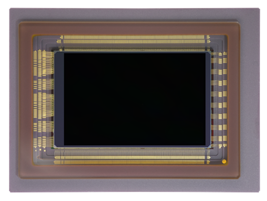
Fig. 2 The GSENSE3243BSI image sensor is offered in both sealed and removable coverglass options to allow for a range of operating temperatures including cooling.
The image sensor has a peak quantum efficiency over 80%, a wide angle response, read noise of 3.3 e- at full speed, and a dark current less than 1 e-/pixel/second at 0℃, approximately a 10x improvement over the popular GSENSE2020BSI sensor.
GSENSE3243BSI is a monochrome sensor available in a 455-pin LGA ceramic package, with options for sealed or removable glass lid. Purchase orders can be placed now for samples and evaluation kits that will start shipping in early March.
The GSENSE3243BSI image sensor will be on demonstration this week at the Photonics West Exhibition in San Francisco, at Gpixel booth #366.
For more information, please contact Gpixel at info@gpixel.com or visit www.gpixel.com.
About the GSENSE sensor family
The GSENSE series is Gpixel’s family of ultra high performance rolling shutter scientific CMOS image sensors. The product line addresses a wide variety of applications with diverse specifications including quantum efficiency over 95%, noise below 1 e-, dynamic range up to 110 dB and data rates over 76 Gbps. Primary applications include spectroscopy, fluorescence imaging, astronomy, high energy physics, UV imaging, medical imaging and high-end surveillance.
About Gpixel
Gpixel is an international company providing high-end customized and off the-shelf CMOS image sensor solutions for industrial, medical, scientific, and professional imaging applications. Gpixel’s standard products include the GMAX and GSPRINT global shutter, fast frame rate sensors, the GSENSE high-end scientific CMOS image sensor series, the GLUX series of high sensitivity sensors for surveillance, the GL series of line scan imagers, the GLT series of TDI imagers, GTOF series of iTOF imagers, and the GCINE series of sensors for professional video and photography. Gpixel provides a broad portfolio of products leveraging the latest technologies to meet the ever-growing demands of the professional imaging market.